Held from October 14 to 16 at the Shenzhen Convention and Exhibition Center (Futian), the WESEMiBAY Semiconductor Ecosystem Expo 2026 brought MANST to Booth 7H08, where the company showcased its glass substrate thin-film process solutions and core equipment, including magnetron sputtering (PVD), atomic layer deposition (ALD), and precision slot-die coating systems.

As demand for AI computing power and high-performance computing continues to grow, advanced packaging is evolving toward larger sizes and higher interconnect densities. Glass substrates have attracted widespread attention due to their excellent dimensional stability, electrical insulation properties, and tunable dielectric constant. TGV (Through Glass Via) is a key structure for achieving electrical interconnection between the upper and lower surfaces of glass substrates and supporting high-density vertical interconnects.
However, the industrialization of glass substrate advanced packaging still faces core process challenges such as metallization of high-aspect-ratio TGV vias, control of film deposition uniformity and continuity, and fabrication of large-area RDL dielectric layers. With three major technology platforms—PVD, ALD, and slot-die coating—MANST covers key processes including uniform deposition for via metallization and RDL dielectric layer fabrication, providing core equipment support for glass substrate advanced packaging.
01 TGV Core Technology: Metallization and Interconnect Reliability
After glass substrates undergo laser modification and wet etching to form vias, a metal adhesion layer and a copper seed layer typically need to be deposited first, followed by copper electroplating filling to form vertical conductive pathways. The continuity of the seed layer and interfacial adhesion performance are key factors affecting electroplating quality and long-term interconnect reliability.
As via diameters shrink and aspect ratios increase, PVD directional deposition is constrained by shadowing effects, resulting in insufficient via sidewall coverage and localized seed layer discontinuity, which can easily lead to electroplating voids and non-uniform filling. Meanwhile, the mismatch in thermal expansion coefficients between glass and metal, as well as residual stress in thin films, further affects interfacial stability.
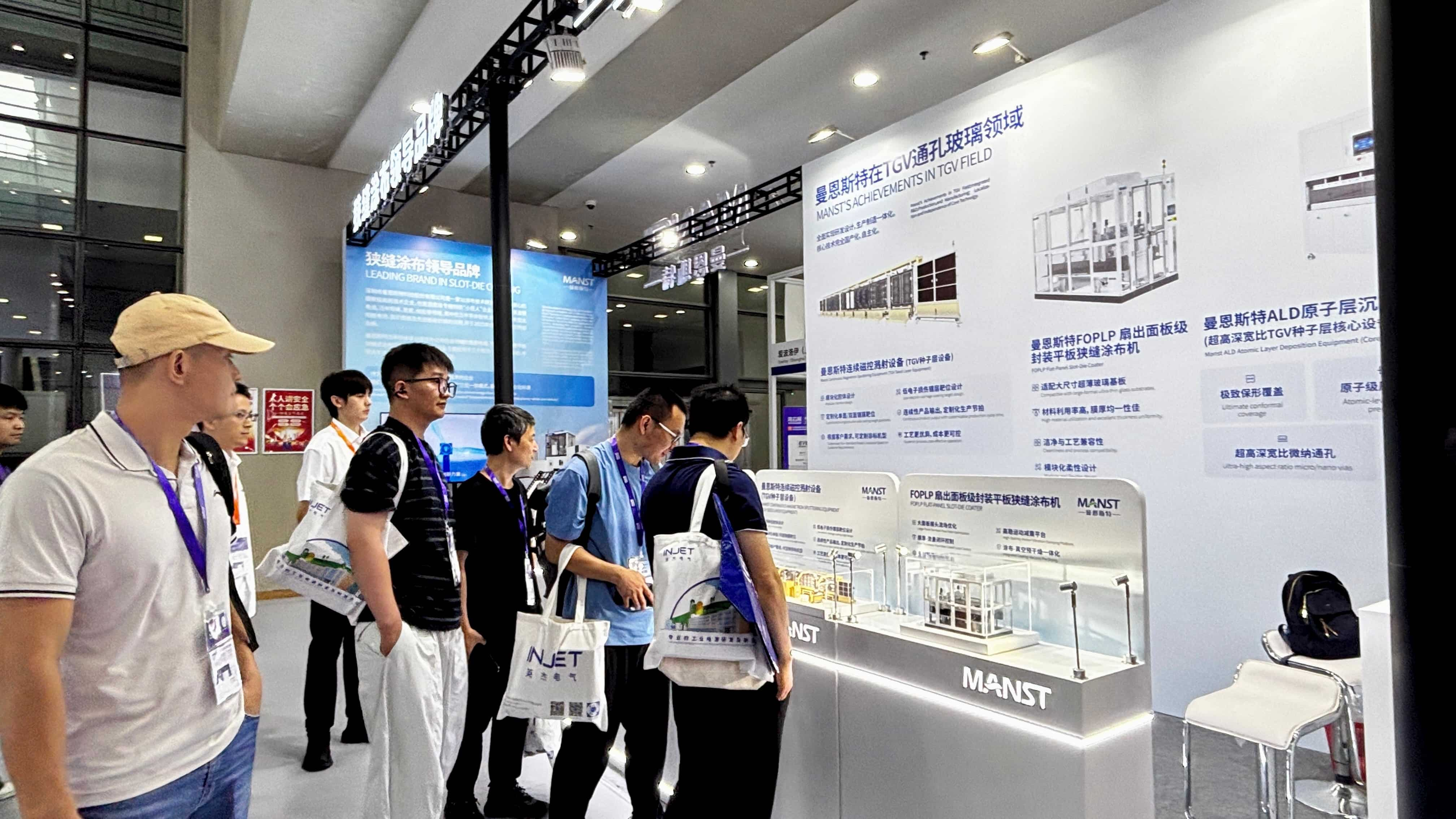
At the exhibition site, MANST's independently developed continuous magnetron sputtering (PVD) equipment and atomic layer deposition (ALD) equipment attracted attention from numerous technical personnel and corporate representatives. Addressing thin film deposition requirements for TGV vias with different diameters and aspect ratios, the two types of equipment form process complementarity: PVD focuses on high-efficiency metal deposition, while ALD focuses on conformal coverage of high-aspect-ratio structures.
Continuous Magnetron Sputtering (PVD): High-Efficiency Deposition of Metal Adhesion Layers and Seed Layers
The equipment adopts a fully automated substrate loading/unloading design, reducing batch waiting time associated with batch-type equipment and effectively improving equipment throughput. It also supports customizable production takt time, providing equipment configurations covering different stages from laboratory and pilot-scale to large-scale mass production.
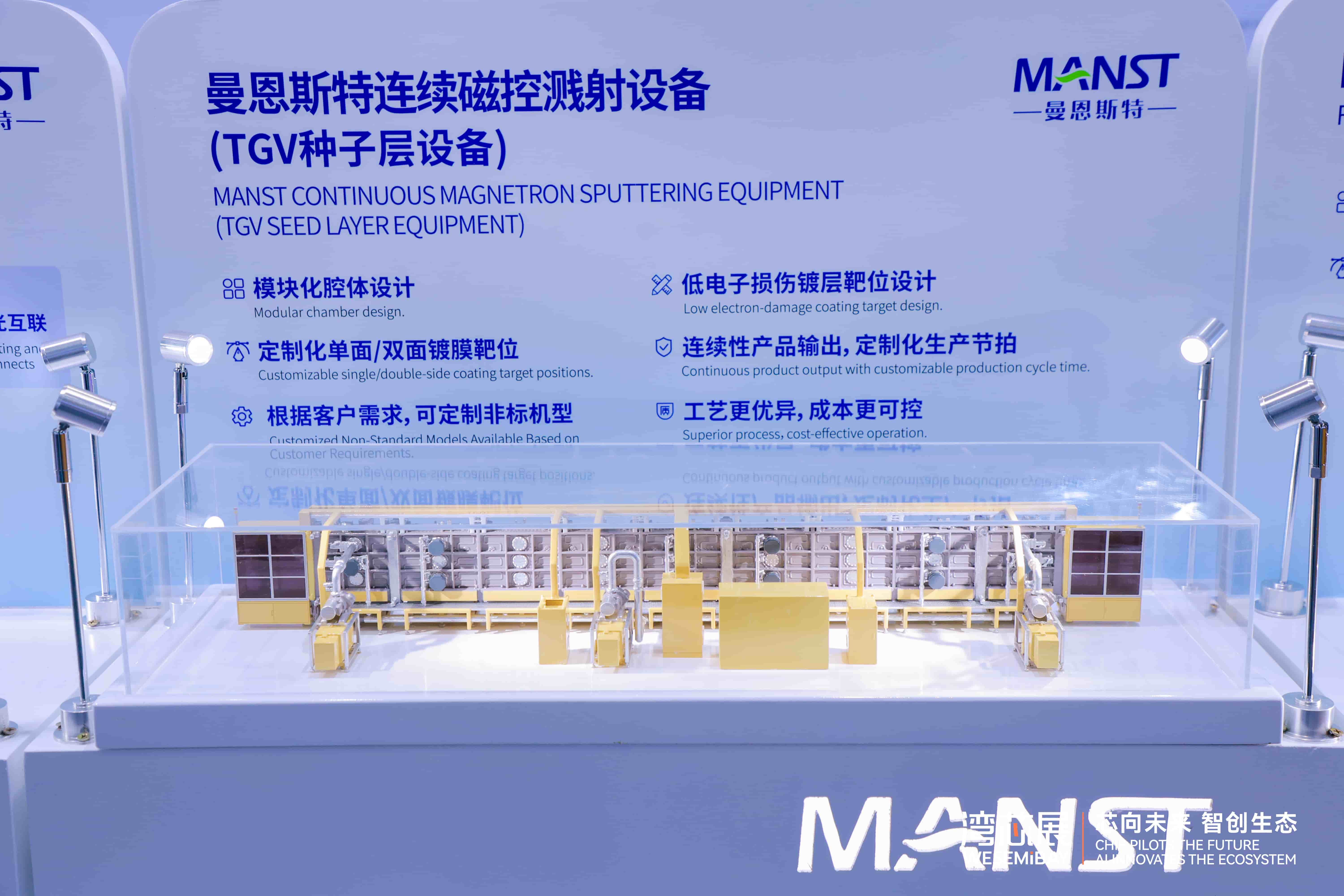
The equipment is equipped with HiPIMS high-power impulse magnetron sputtering technology, which enhances metal thin film density and interfacial adhesion by optimizing plasma characteristics. Targeting the thermal load sensitivity of glass substrates, it adopts low-temperature deposition and low-damage process design, effectively suppressing warpage of ultra-thin glass substrates and ensuring uniform and dense coatings. The equipment addresses via metallization requirements with aspect ratios ≤ 12:1 and is compatible with various substrates including glass, ceramics, and silicon-based materials.
Through modular chamber design, it supports customization of single-sided or double-sided coating target positions, balancing process configuration flexibility and maintenance convenience. Combined with a continuous production mode to reduce batch switching losses, it helps customers optimize unit output costs.
ALD Atomic Layer Deposition: Thin Film Deposition for High-Aspect-Ratio Structures
The ALD equipment is based on self-limiting surface reactions, achieving atomic-level film thickness control, with excellent film uniformity and process repeatability, thoroughly eliminating structural shadowing effects. It is suitable for fine preparation of functional thin films such as barrier layers, interface layers, and conductive nucleation layers in high-aspect-ratio vias.
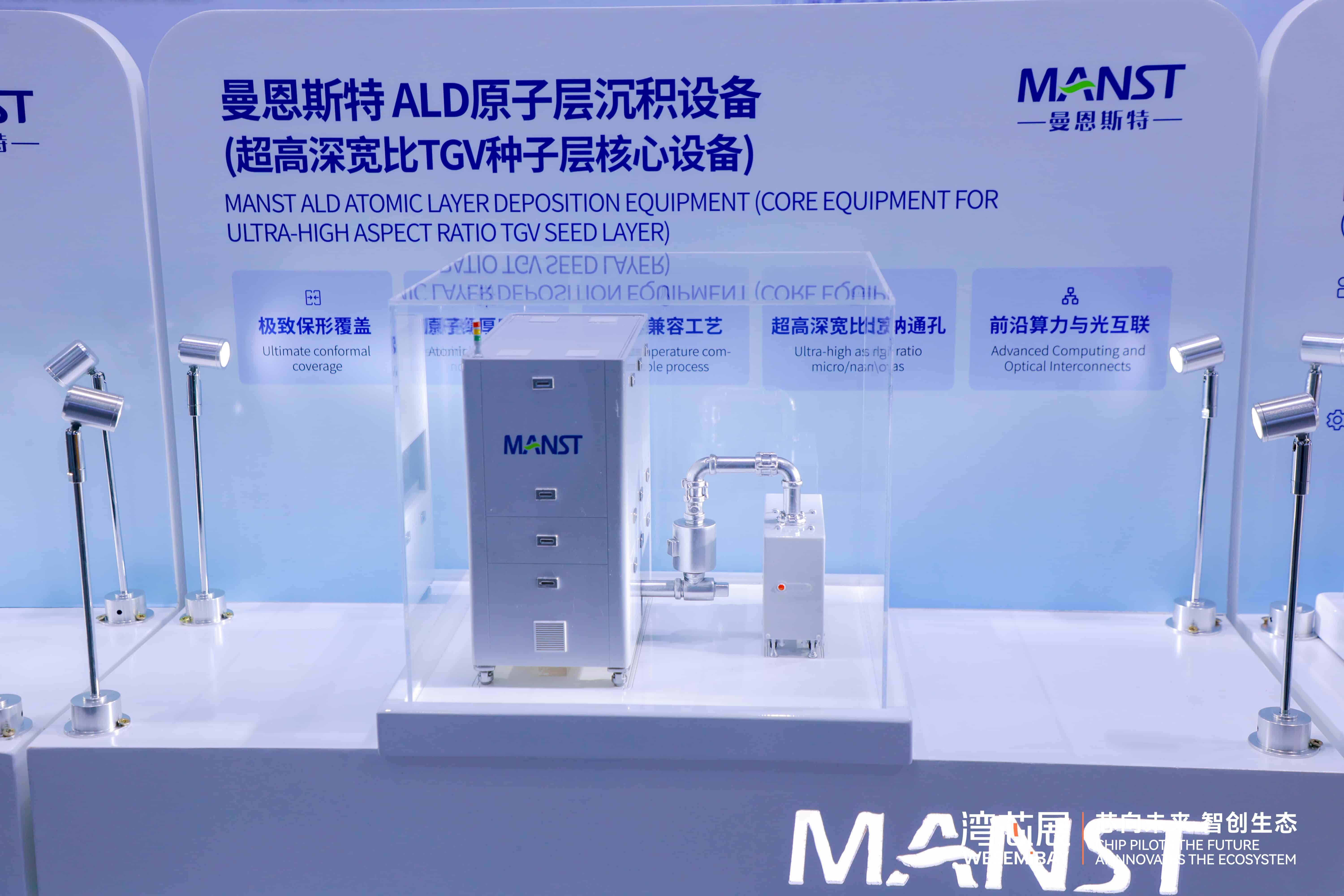
The equipment supports high-aspect-ratio via applications with aspect ratios of 15:1–150:1 and via diameters below 20 μm. Under suitable process conditions, step coverage is nearly 100%, providing technical support for functional thin film preparation of complex three-dimensional structures.
Meanwhile, the mild process temperature is compatible with a variety of heat-sensitive substrates, reducing thermal load while ensuring film formation quality, and helping to reduce the risk of thermal deformation and performance degradation in glass substrates.
From high-efficiency metallization at conventional aspect ratios to conformal deposition at ultra-high aspect ratios, PVD and ALD form gradient coverage, providing differentiated technical options for different TGV structures.
02 RDL Dielectric Layers: Slot-Die Coating Enhances Large-Area Film Uniformity
As glass substrate advanced packaging develops toward large sizes and panel-level manufacturing, traditional spin-coating processes face challenges in material utilization and film thickness uniformity. MANST's flat-panel slot-die coating equipment adopts a linear coating method without rotational mechanical stress, supports single-sided and double-sided process switching, and provides high-uniformity, low-loss coating technology support for large-area photosensitive PI/PBO dielectric materials and photoresist coating.
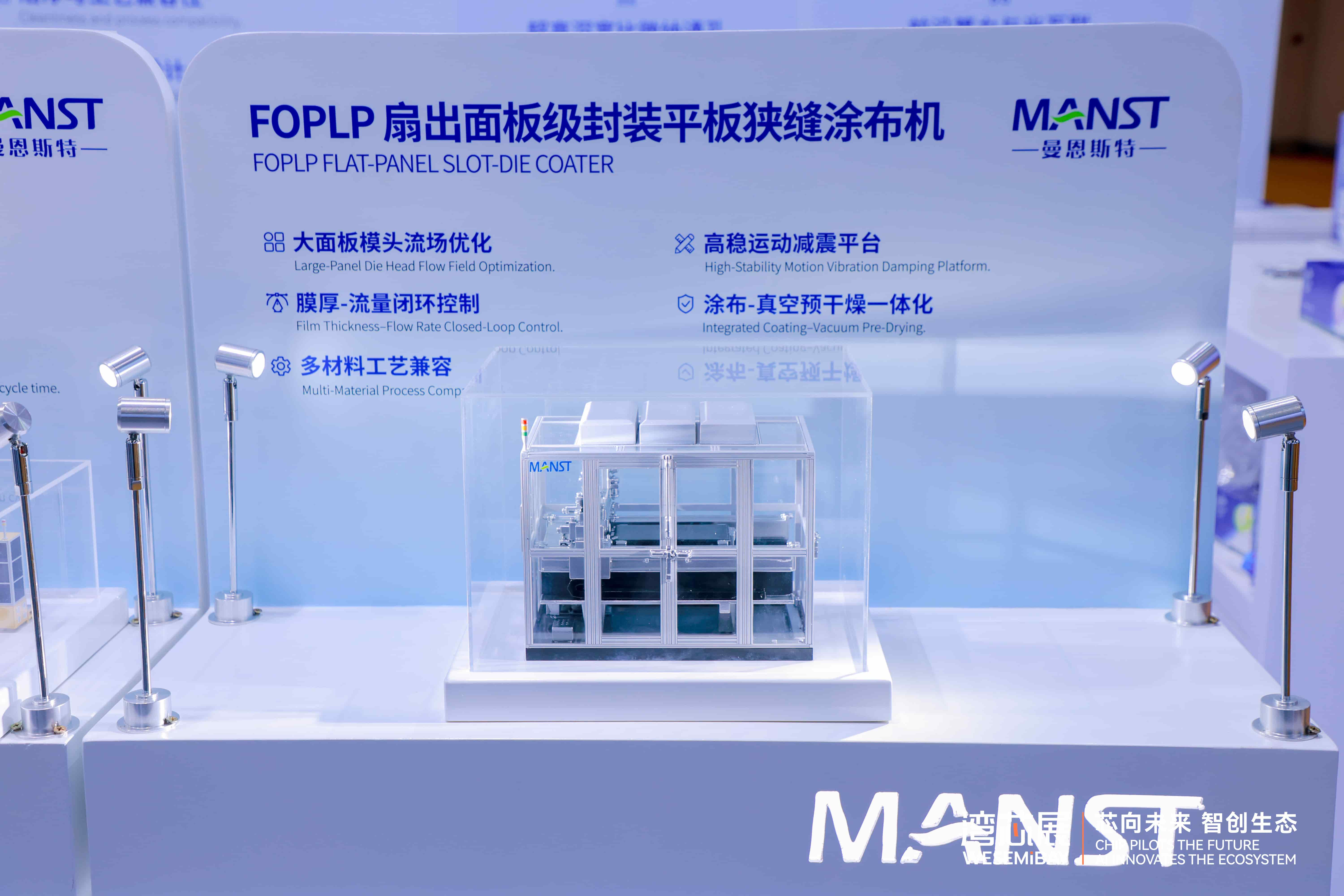
High-Precision Film Formation Ensures Dielectric Layer Uniformity
The equipment is equipped with a self-developed high-precision coating die and closed-loop liquid supply system, achieving film thickness uniformity ≤ 3% in the effective coating area and material utilization > 95%, providing a critical process foundation for uniform preparation of dielectric layers required for fine circuitry.
Stable Liquid Supply and Cleanliness Control Reduce Coating Defect Risk
The high-precision injection pump achieves a flow rate resolution of 0.01 μL/s. Combined with die pre-extrusion, automatic cleaning, and a whole-machine FFU cleanliness system, it effectively improves liquid supply stability and cleanliness control during coating, reducing the risk of coating defects caused by residual liquid and particle contamination.
Multi-Material Compatibility Supports Scalable Manufacturing
The equipment is compatible with borosilicate glass substrates of various specifications and semiconductor dielectric materials, supporting model selection from small-batch R&D to panel-level mass production, and providing dielectric layer preparation process support for L/S 2–5 μm RDL fine-line patterning.
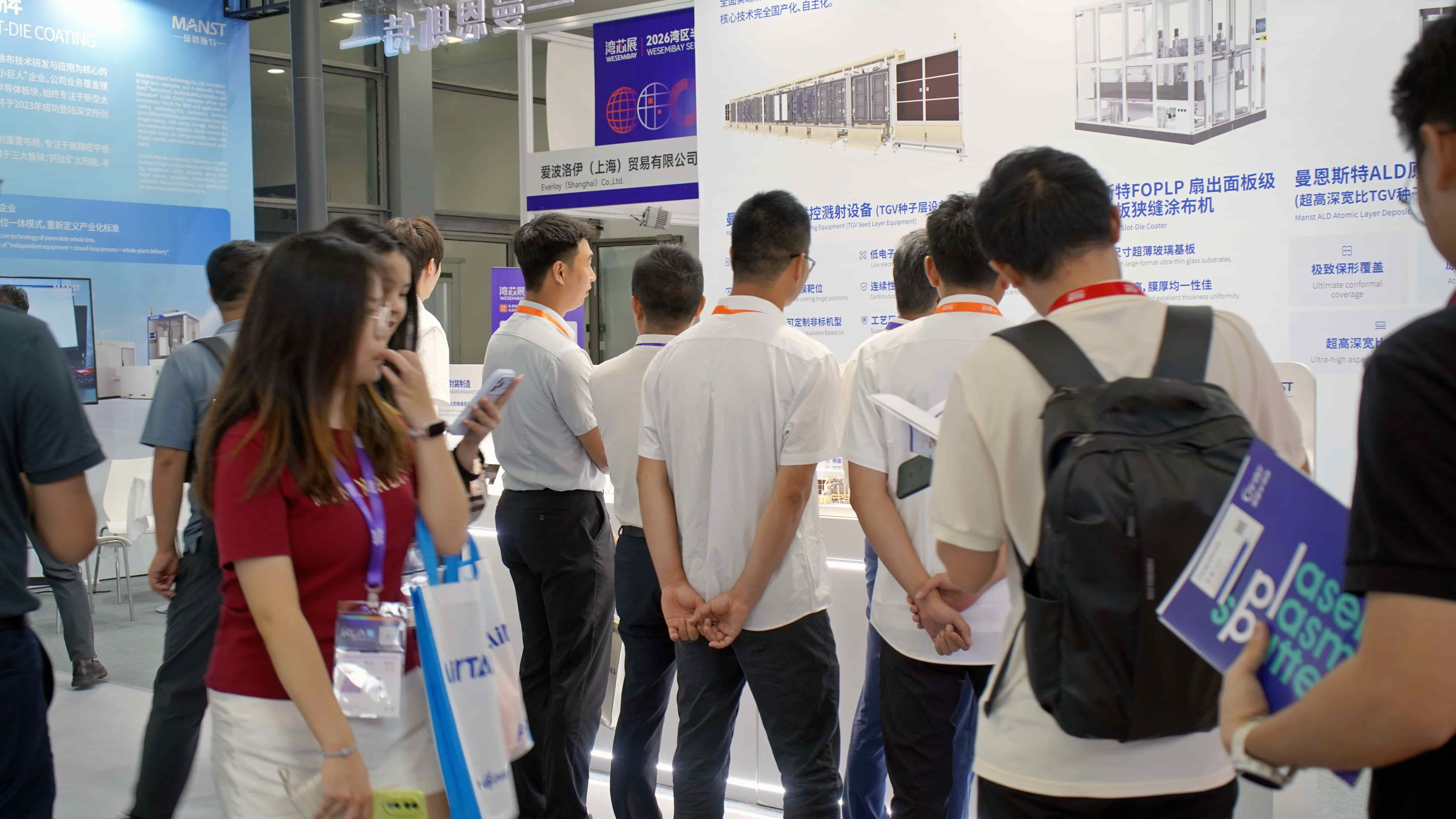
During WESEMiBAY 2026, MANST held in-depth discussions with industry peers on process challenges, technological developments, and the commercialization of glass-substrate advanced packaging.
Looking ahead, as demand grows in areas such as AI computing, CPO optical interconnects, and 2.5D/3D advanced packaging, MANST will continue to advance core process and equipment technologies and explore new applications, supporting the further development and adoption of glass-substrate advanced packaging.
NO.3, Zhukeng Third Industrial Zone, Jinniu East Road, Pingshan District, Shenzhen
0755-89369630
400-822-5968
brand@sz-manst.com